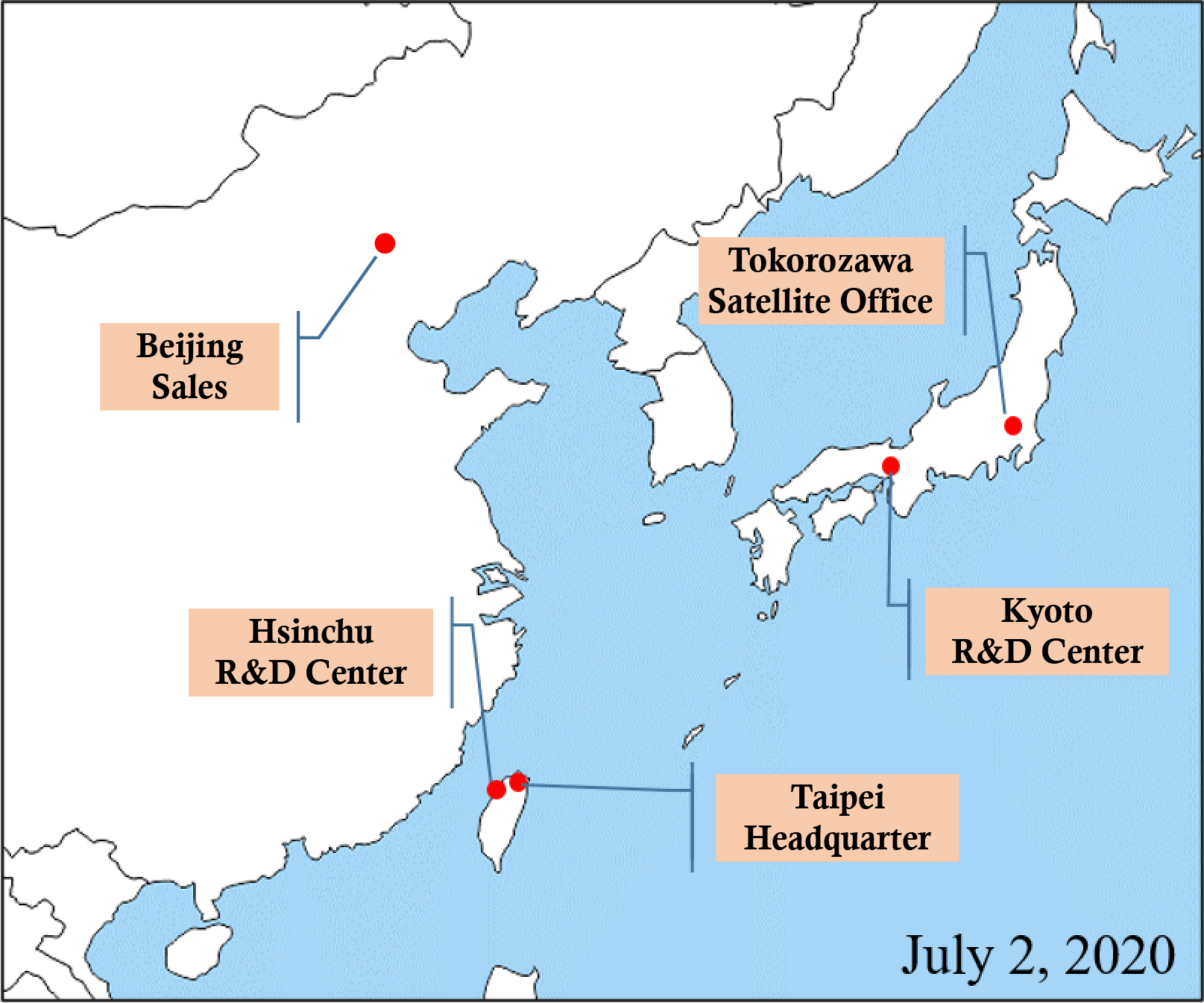
MISSION

As global warming becomes a serious problem, reducing the emission of carbon dioxide and saving energy is an important social issue and the development of green energy technology becomes essential as well. Paradigm shift of green technologies is ongoing. Boosting energy efficiency for the infrastructure of vehicle, railroad, smart grid and etc. is indispensable.

ANJET Corporation endeavours to develop semiconductors that can enhance the energy efficiency for the sustainability of the society.

We work together with IC foundries in Taiwan, Japan and US to design the competitive power devices leveraging Si, SiC and GaN processes for every kind of applications.

ABOUT US

Taipei ANJET Corporation
Establishment date:
September, 6th, 2019
Address:
5F-6, No. 308, Zhifu Rd., Zhongshan Dist., Taipei City 10466, Taiwan R.O.C.
Capital:
390,000,000 NTD
Team:
Each has affluent experience of 20-30 years in Semiconductor Industry, namely Texas Instruments, Mitsubishi Elec., Renesas, and ROHM
Offices:
  • Taipei ANJET Corporation
    • Taipei Headquarters
    • Hsinchu R&D Center
  • Anjet Research Lab Co., Ltd.
    • Kyoudai Katsura Venture Plaza
    • Tokorozawa Satellite Office
  • Beijing Sales
Business:
Research and development(R&D) and sales of semiconductor component
Anjet Research Lab Co., Ltd.
Establishment date:
December 3, 2019
Address:
2203,2208 South Building, Kyodai-katsura Venture Plaza, 1-39 Goryo Ohara, Nishikyo-ku, Kyoto-city, kyoto-prif., 615-8245, Japan (Map)
Supported by
JETRO Kyoto
Capital:
70,000,000 JPY
Team:
It consists of some expert members with experience in research and development of power semiconductor devices and modules at major semiconductor manufacturers.
(Texas Instruments, ON Semiconductor, UMC, Hitachi, Mitsubishi Elec., Renesas, Panasonic, ROHM etc.)
Business:
Design of Semiconductor Devices

PRODUCT

SiC SBD 650V-1200V (2A~20A)
...
Key features
  1. Best-in-class low VF:1.35V
  2. High surge ruggedness
  3. Temperature independent switching behavior
  4. Low cost
  5. High reliability
Key technologies
  1. Advanced junction barrier schottky structure
  2. Advanced termination structure
  3. thin Wafer
SiC DMOS 650V/1200V (100mΩ~20mΩ)
...
Key features
  1. Best-in-class low Rsp:≒3.3mΩ・cm2
  2. Enough break down voltage
  3. Low Cgd
  4. Low cost
  5. High reliability
Key technologies
  1. Advanced DMOS self-align structure
  2. Advanced termination structure
  3. thin Wafer
...

RECRUIT

Job description

【R&D engineer】(SiC、GaN)
  1. Familiar with power semiconductor device design (SBD, DMOS, Trench MOS, IGBT)
  2. Familiar with EDA Tool (Such as Synopsys Sentaurus)
  3. Fluent in English or Japanese
【Power Module design】(SiC、GaN)
  1. Familiar with power semiconductor package and module design
  2. Fluent in English or Japanese

simulation ①

simulation ②